|
|
|

|
|||||
|
|
|
Intel will be the first chipmaker to use high-NA EUV lithography, giving it a potential advantage over TSMC.
The company has long pointed to its 14A node in 2028 as the first node in which it will use high-NA.
However, there have been hints Intel may insert high-NA earlier into its 18A node, which is ramping up today.
There's a conventional wisdom among investors that Intel (NASDAQ: INTC) is significantly behind Taiwan Semiconductor Manufacturing (NYSE: TSM), and that it will take years for the company to catch up to TSMC's technological lead -- if it ever happens at all.
Last week, sell-side analyst Stacy Rasgon of Bernstein said that since it took a decade to "break" Intel, investors shouldn't expect it to take less than 10 years to fix. Notwithstanding Intel's heavy lift turnaround really began in 2021 with the appointment of former CEO Pat Gelsinger, the turnaround may actually be closer than Rasgon expects.
Where to invest $1,000 right now? Our analyst team just revealed what they believe are the 10 best stocks to buy right now. Continue »
One key element for Intel being able to leapfrog TSMC would be the earlier implementation of high-NA EUV lithography technology. While Intel has publicly stated that it won't introduce high-NA until its 14A node in 2028, there were numerous indications over the past year that Intel may in fact accelerate HNA into its current 18A manufacturing process.
If that happens, the semiconductor industry could change very quickly.
High-NA EUV lithography is the latest and most advanced version of extreme ultraviolet lithography technology (EUV), pioneered and developed by ASML Holdings (NASDAQ: ASML). Twenty years in the making, chipmakers first used EUV lithography in 2019, enabling the efficient production of chips with pitches as small as 7 nanometers between transistors.
About a decade ago, Intel delayed its implementation of EUV, instead opting for double, triple, or even quadruple patterning with older DUV technology. That delay allowed TSMC to leapfrog Intel, giving the Taiwanese giant a manufacturing lead it has held to this day.
High-NA is the next jump forward in this technology. HNA EUV machines can "write" chip patterns in a thickness of just 8nm, more precisely than the 13.5-nm light beams of low-NA EUV. Like its predecessor, the new technology enables single-patterning, higher-density chips with fewer process steps. Fewer process steps generally means higher yields than multi-patterning with older tools.
Determined not to repeat mistakes of the past, Intel has jumped to the front of the line as the first to implement high-NA EUV machines. Ironically, it's TSMC this time that has opted to wait to use the new technology, with TSMC management citing cost reasons.
But both Intel and ASML have claimed that high-NA machines are working as intended now. In early 2024, ASML's CEO took issue with critics of HNA, saying it is "very clearly the most cost-effective solution both in logic and memory."
Then at a technology conference in February 2025, Intel executive Steve Carson noted Intel already had HNA "in production," and that the tool was "more reliable" at this stage than low-NA was at the equivalent time in the past. Carson also noted high-NA enabled Intel to do the same work with one machine and a "single-digit" number of process steps that it took a low-NA machine three exposures and roughly 40 processing steps. So, there appear to be clear advantages for HNA in terms of productivity, especially when one gets to leading-edge nodes that require triple-patterning on low-NA tools.
Now, there are technology obstacles to using HNA tools effectively, and the tool costs about double that of a low-NA tool. Still, given the productivity enhancements, HNA lines should net out to overall cost savings when properly implemented.
Another reason Intel may be ready to use HNA EUV today is that it has already bought, installed, and utilized at least three tools it has disclosed to the public, and possibly more that it hasn't.
Intel announced the receipt of its first HNA machine at its Oregon R&D facility in late 2023/early 2024, then announced "first light" on the machine in late February 2024. Intel next followed that up with the disclosure of a second HNA machine installation in August 2024 at its Oregon facility.
Then, just two weeks ago in mid-December, Intel announced it had achieved "acceptance testing" of ASML's EXE:5200 HNA machine, the upgraded version of last year's EXE:5000 high-NA machine, which features enhanced throughput for high-volume manufacturing. Acceptance testing means Intel has the HNA machine working in the fab, meeting high-volume manufacturing benchmarks and customer specifications.
Notably, ASML didn't start shipping the 5200 until early 2025, indicating that Intel has at least one more than the two it officially announced in 2024. In addition, Intel has not disclosed specifically where the third machine, the 5200, was installed. Notably, Intel has been preparing Fab 52 in Arizona for 18A production this year.
It's also quite possible, if not probable, that Intel has purchased even more HNA machines. In May 2024, industry publication The Elec reported that Intel had secured all of ASML's high-NA EUV production for 2024, which would encompass five to six machines. Given Intel received its first machines in late 2023, that would bring its total to six or seven.
This was just one unconfirmed report, and Pat Gelsinger's resignation in late 2024 may have changed this order pattern. Nevertheless, it's likely a fair bet that Intel has purchased more than the three HNA machines it has officially disclosed.
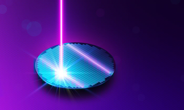
Image source: Getty Images.
In light of all this, it's curious Intel has pointed to 14A, due out in 2028, as the point in which it will use high-NA. And it's especially curious that Intel would purchase so many HNA machines, given that this past summer, Intel disclosed that if it doesn't secure a significant external customer, it might not proceed with 14A development at all.
If Intel weren't sure it would develop 14A, and since it has pointed to 14A being the first HNA node, why would Intel buy so many expensive HNA machines, which cost $400 million each? And why would it do so when the company was already cash flow negative, to the point where the company took in dilutive equity investments this past summer?
Intel has also already accomplished a tremendous amount of work with HNA tools. At the February tech conference I mentioned, Intel disclosed that it was processing 30,000 wafers per quarter on high-NA tools. That's a huge number of wafers to be processing for mere research and development purposes. Meanwhile, the recent disclosure of "acceptance testing" means that the tool has passed a formal evaluation process that determines the tool can function according to contractual specifications in a formal manufacturing setting.
Since the tool appears to be working in manufacturing settings, Intel has extensive experience with it, and HNA reportedly provides material advantages, why wouldn't Intel integrate HNA into the current 18A process?
While Intel has obviously never said it would use high-NA EUV for 18A, the company has nevertheless dropped clues it would be possible to do so over the past year. Meanwhile, outsiders have begun to speculate over the possibility of high-NA machines in Fab 52.
Reporting on the aforementioned February 2025 technology conference, Reuters initially reported that Intel was developing 18A with high-NA technology; however, Intel later had Reuters correct the story to say that Intel was "using its 18A manufacturing technology, which is scheduled for mass production with a new generation of PC chip later this year, to test the high NA tools."
So, Intel was at least "testing" high-NA on its 18A process as of February.
Then at Intel's Foundry Direct event in April, Intel's chief technology and operations officer Naga Chandrasekaran stated that Intel had achieved "yield parity" between testing both low-NA multi-patterning and high-NA single-patterning on both the 18A and 14A nodes.
More recently in October, Intel invited technology journalists into Fab 52 for Intel's "Tech Tour" to show off the fab and its 18A node. While all of the journalists were under nondisclosure agreements, a vlogger for Level1Techs told his viewers that he saw "something" in Fab 52, asked about it, and was told by Intel to please refrain from disclosing what he saw.
I did notice a few things that raised some interesting questions. Which I asked. And that's why I later got the polite email encouraging me to, uh, you know, um, 'not notice' things so specifically.
During this portion of the vlog, the Level1 presenter showed a video of the original HNA machine being installed in Oregon. After discussing the EUV machines he saw, without specifying the model, the presenter said, "That's probably the extent of the detail I'm comfortable giving you."
For the record, there's no evidence that Intel is using HNA EUV on 18A. But given its purported advantages, why keep it a secret if it were?
There could be a number of reasons. One might be the competitive advantage of keeping cards close to the vest, surprising the competition and thereby lengthening Intel's first-mover advantage with HNA. There may also be a concern over setting expectations too high for cost savings, yield, and performance with the first incarnation of the tool's use. After all, numerous rumors were circulated about Intel and 18A's progress over the past year, with many being quite negative.
Additionally, even if Intel does use high-NA tools for 18A, it may only do so on a few layers of each chip. Current leading-edge 3nm-class chips include about 20 EUV layers, and it's expected upcoming 2nm-class chips, of which 18A is a part, will see that EUV layer count jump by 30% into the mid-20s.
Moreover, a recent short documentary about Fab 52 by CNBC appeared to show low-NA EUV tools in the fab. Therefore, even if HNA is used on 18A, it may only be for certain products, or perhaps only for a few critical layers, with the majority still handled by low-NA tools.
Thus, Intel may be wary of labeling 18A a "high-NA" node if most layers are still completed using low-NA tools. It's also possible that Intel may be using low-NA tools for 18A, but will actually insert HNA tools for the next variant of the node called 18AP, which is supposed to ramp later in 2026 and deliver an 8% improvement in performance-per-watt over 18A.
Investors may never know whether Intel is actually using HNA tools on 18A, given the secrecy that generally accompanies semiconductor manufacturing. If Intel does choose to disclose it, next week's CES in Las Vegas could be the ideal time and place, given that Intel will formally unveil its first 18A-produced chip, called Panther Lake.
Nevertheless, given the company's tight-lipped posture regarding the 18A process, it may very well remain a mystery as to whether Intel is using high-NA EUV for its critical 18A node.
Before you buy stock in Intel, consider this:
The Motley Fool Stock Advisor analyst team just identified what they believe are the 10 best stocks for investors to buy now… and Intel wasn’t one of them. The 10 stocks that made the cut could produce monster returns in the coming years.
Consider when Netflix made this list on December 17, 2004... if you invested $1,000 at the time of our recommendation, you’d have $505,749!* Or when Nvidia made this list on April 15, 2005... if you invested $1,000 at the time of our recommendation, you’d have $1,149,658!*
Now, it’s worth noting Stock Advisor’s total average return is 979% — a market-crushing outperformance compared to 195% for the S&P 500. Don't miss the latest top 10 list, available with Stock Advisor, and join an investing community built by individual investors for individual investors.
*Stock Advisor returns as of January 1, 2026.
Billy Duberstein and/or his clients has positions in ASML, Intel, and Taiwan Semiconductor Manufacturing. The Motley Fool has positions in and recommends ASML, Intel, and Taiwan Semiconductor Manufacturing. The Motley Fool has a disclosure policy.
| 5 min | |
| 7 min | |
| 1 hour | |
| 1 hour | |
| 1 hour | |
| 1 hour | |
| 2 hours | |
| 2 hours | |
| Jul-20 | |
| Jul-20 | |
| Jul-20 | |
| Jul-20 | |
| Jul-20 | |
| Jul-20 | |
| Jul-20 |
Join thousands of traders who make more informed decisions with our premium features. Real-time quotes, advanced visualizations, alerts, and much more.
Learn more about Finviz Elite